


1 引言
Z源变换器是Michigan State University的彭方正教授2002年提出的一种功率变换器拓扑,能够调节直流母线电压[1]。Z源变换器和DC-DC变换器都能够调节逆变器的直流母线电压,但Z源变换器用到的有源器件更少,可靠性更高。其自提出以来受到了研究人员的充分重视,人们开展了大量的研究工作,内容涉及变换器主电路参数设计,主电路拓扑改进,变换器 PWM 调制策略,Z源整流,Z源逆变,Z源网络和矩阵变换器相结合,Z源网络和多电平变换器相结合等方面。应用涉及电机调速[2]、光伏发电[3,4]和电动汽车[5,6,7,8,9,10]等诸多领域[5,11-14],本文只做Z源逆变方面的讨论。
2 Z源逆变器具备的优势及其发展脉络
Z源网络由两对对称的电感、电容和一个输入侧二极管构成,如图1所示。通过三相桥臂在不同状态的切换,完成电感电容的充放电控制,使得直流链电压在逆变桥非直通状态得到泵升,达到升压的目的。按照开关管的导通状态,Z源逆变器的工作状态可以分为两大类——直通状态和非直通状态。直通状态时,至少有一路桥臂的上下两路开关管同时导通,也就是通常所说的“桥臂短路”。一般按桥臂直通数目,直通方式可以分为单相、两相和三相直通。非直通状态也即传统电压源型变换器所具有的工作状态,包括零状态和有效状态。
图1
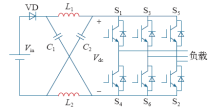
非直通状态期间,输入侧二极管导通,电感向电容放电;直通状态期间,由于二极管阴极电压高于阳极电压,故其处于关断状态,Z源网络电感被电容充电。
假设Z源逆变器输入直流电压为Vin,直通占空比为ds(0<ds<1),可以推得直流链电压Vdc为
由式(1)可以看出,Z源逆变器实现了电压泵升。相比于电压型逆变器及DC-DC+逆变器升压结构,具备以下几点优势:
(1)Z源逆变器融合了电压源电容恒压和电流源电感恒流的优势,允许电压型逆变器桥臂短路,电流型逆变器桥臂开路,提高了功率变换器的可靠性。
(2)相比于DC-DC升压拓扑,Z源逆变器拓扑为单级结构,控制上更容易实现。
(3)传统变换器为了避免桥臂直通,通常的做法是在驱动输出中加入死区,而为了减小死区造成的不利影响,往往又需要加入死区补偿,增加了控制难度。Z源逆变器允许直通,从根本上消除了由死区带来的影响。
(4)相对于DC-DC变换器,Z源网络需要的有源器件更少(单向变换器不需要,双向变换器需要1个),可靠性更高。如果网络中2个电感采用耦合技术,那么Z源变换器的成本会比DC-DC变换器低。
Z源变换器提出伊始,大家普遍致力于直通调制策略的研究,力求在相同的直通占空比下升压比更高、器件应力更小、实现更为简单且电感电流纹波更小。随着Z源逆变器的逐步发展,学者们开始探索将其应用于诸如电动汽车、光伏发电和电机调速等领域,使得Z源逆变器的应用领域更加宽阔。而贯穿Z源逆变器发展至今,Z源变换器拓扑结构及控制方式一直为大家的研究热点。针对应用对象的不同,学者们对新变换器拓扑的探索脚步从未停止,不断地提出诸如器件数目少、体积小、升压比高及启动冲击小的新变换器结构。在控制方式上,Z源逆变器刚被提出时,应用最多的为简单易实施的开环控制。随着Z源变换器应用领域的逐步推广,客观上对变换器性能的要求越来越高,单闭环、双闭环控制策略开始逐步取代开环结构;另外,滑膜控制、模糊控制等智能控制策略也被尝试着应用于Z源逆变器。以下从拓扑结构、调制方式和闭环控制策略三个方面展开讨论。
3 拓扑结构的研究
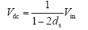
3.1 以减小网络电压应力为目的的拓扑
图2
由于输入电流连续,输入电流连续电压型准Z源网络更容易进行输入侧滤波,用于蓄电池等供电的场合,在光伏并网系统中可以省略输入滤波环节。电容C1的电压应力和传统Z源网络相同,而电容C2的电压应力减小至原来的ds倍。输入电流断续电压型准Z源网络输入电流断续,但两个电容承受的电压都大幅降低,为原来的ds倍。
图3
3.2 以减小电感/电容数目为目的的拓扑
考虑到Z源网络的两个电容和电感占据的大空间和重量,学者们对此展开了研究,提出了以下几种类型的Z源逆变器。
图4中所示的是变压器或电感耦合技术的几种Z源逆变器。Trans-Z源[18]和Γ-Z源逆变器[19]以双绕组变压器的形式来替代传统Z源逆变器中的两个电感,将电感和电容的数目都降为1。Trans-Z源在保持高升压比的同时也保证了低电压应力的优势。与其他由变压器或耦合电感构成的逆变器不同的是,随着电压比的增大,Γ-Z源逆变器的升压比会逐渐变小。T-Z源逆变器[20]采用了双绕组电感耦合的技术,同样将电感和电容的数目降低至1。由于无源器件和逆变器共用一个直流源,这种结构的阻抗网络很适合于在多电平NPC逆变器中应用。使用变压器或电感耦合技术的Z源逆变器虽然在结构上使得电感和电容的数目减小,但在工程技术上却难以避免由漏感带来的不利影响[21,22,23,24]。
图4
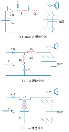
图5
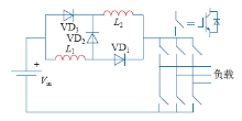
图6
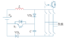
图7为该拓扑在反并联二极管后带不同负载时的波形,从图中可以看出,电感电流断续,并且负载不同时,导致的直流链电压值也不同。这既不利于负载侧控制,也给主电路器件带来过电压危险,故该种拓扑的逆变器更适合工作于负载固定或变化范围很小的场合。
图7
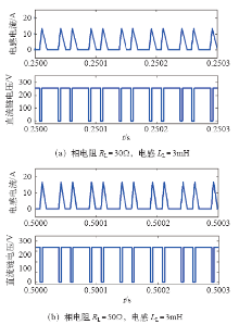
图7
带反并联开关管时电感电流和直流链电压波形
Fig.7
Inductor current and DC-link voltage waveforms with anti-parallel switch
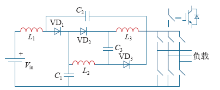
3.3 以提高升压比为目的的拓扑
图8
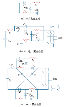
图9
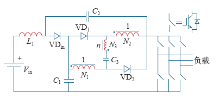
采用变压器或耦合电感结构,通过改变绕组匝数比来达到进一步升压目的的Z源逆变器拓扑也有很多,之前所述的Trans-Z源逆变器和T-Z源逆变器就是这种结构。当匝比大于1的时候,它们的升压比都要比传统Z源逆变器高。
图10
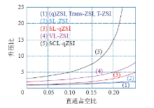
以n来表示耦合电感的匝比,附表展示了所述的几种典型的Z源逆变器在升压能力和器件数目方面的特性。
表 几种Z源逆变器对比
Tab.
| 名 称 | 升压比 | 二极管 /个 | 电容 /个 | 电感/个 | 特 性 |
|---|---|---|---|---|---|
| (q)ZSI | 1 | 2 | 2 | 控制简单,可靠性高;升压比低;存在启动冲击问题 | |
| Trans-ZSI 和T-ZSI | 1 | 1 | 2绕组变压器或耦合电感 | 体积小;升压比高;输入电流断续 | |
| SL-ZSI | 7 | 2 | 4 | 升压比高;器件数目很多;可靠性低 | |
| SL-qZSI | 4 | 2 | 3 | 升压比高;器件数目多;二极管电压应力大 | |
| VL-qZSI | 3 | 3 | 3 | 升压比高;电容电压应力大 | |
| SCL-qZSI | 3 | 3 | 1个独立电感和一个三绕组耦合电感 | 升压比极高;电容电压应力大 |
图11
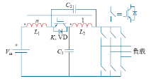
3.4 其他类型拓扑
图12
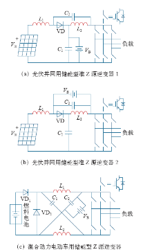
图13
4 直通实现方式的研究
基于SPWM控制方式下的3种调试方式中,简单SPWM控制最为简单,但升压空间有限,器件的电压应力大;最大SPWM控制实现了升压最大化,但由于直通占空比不定,电感电流和电容电压存在6倍纹波分量,增加了电感和电容的设计指标;最大恒定升压比SPWM控制升压比比最大SPWM控制略小,但其直通占空比恒定,电感设计值更小,在SPWM调制方式中综合性能最优。
同SPWM控制方式相比,SVM方式具有更多的优势,如更高的电压利用率,更低的电流谐波含量和开关损耗,是目前应用最为广泛的方式。按照直通状态的插入时刻和作用时间,存在不同的SVM策略。简单SVM实现简单,但缺点是电感电流脉动大,电感设计指标大,并且开关频率成倍增加,开关损耗大[37]。
从能够实现升压最大化并且不提高开关频率的角度而言,SVM策略主要有两种:直通矢量平均分配的六段式SVM调制 (SVM6)和四段式SVM调制(SVM4),如图14所示,图中,以Tsh表示总的直通时间,以下标“+”,“-”来区别上、下桥臂开关管,以Ta+,Tb+,Tc+,Ta-,Tb-,Tc-来表示Z源逆变器三相桥臂开关管导通和关断的转换时刻。在一个控制周期内,对于 SVM6,总的直通状态被平均分成六等份;而对于SVM4,总的直通状态被平均分成四等份注入到传统零矢量中。
图14
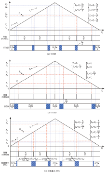
SVM控制下电感电流纹波不恒定,它随着电压矢量相位的变化而变化,并在某些角度处取得最大值。文献[38]详细推导并对比了SVM6和SVM4两种调制方式下电感电流纹波,结论为SVM4方式下的最大电感电流纹波比SVM6方式下的更小。在平均电流和电感量一定的情况下,电流纹波越小,电感体积就越小,应用SVM4策略更有利于减小电感体积。
5 闭环控制方法的研究
Z源逆变器实现控制的核心目的在于调节直通占空比,使直流链电压按照期望值输出。按照反馈变量的类型,分为直接控制和间接控制方法。
直接控制方式采集的反馈参数即为直流链电压,如图15所示。较间接控制方式而言,直接控制方式具有良好的动态响应特性。但是,由于直流链电压为高频脉冲输出,信号不易采集,硬件实现复杂。
图15
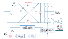
图16
图17
控制算法上,Z源逆变器沿用了传统的PID算法、模糊控制、非线性控制和模型预测控制等,结合算法本身的优势提高了Z源逆变器闭环控制特性。控制模式上可分为电压模式和电流模式[43]。电压模式即为通常所说的单闭环控制,通过采集电压值与给定值取偏差,经过一定的控制算法,最终求取直通占空比。电流模式即为双闭环控制,外环为电压环,内环为电感电流环。电流模式具有优良的稳态和动态特性,另外也抑制了Z源逆变器启动冲击的问题。
6 面临的挑战和未来发展方向
6.1 调制比和直通占空比相耦合,升压比受限
Z源逆变器的调制比m和直通占空比存在以下耦合关系

要想实现升压的更大化,就必须以牺牲m,降低负载波形质量为代价。虽然目前已有多种Z源的衍生拓扑出现,提高了变换器的升压比,但是调制因子和直通占空比的耦合关系依然无法摆脱。
6.2 Z源网络占据空间大,不利于集成
Z源网络中需要2个电感和电容,比DC-DC变换器多一个电感。在大功率控制器中,电感占据的体积和重量是很大的,不利于在电动车等重视控制器重量的场合应用。再者,Z源网络中电感的工作频率和逆变侧的开关频率是一致的。我们知道,控制器的功率越大,为了减少开关损耗,采用的开关频率就越低。而开关频率越低,电感的高频纹波电流就会越大,为避免饱和,就得增加磁芯体积和线圈半径,最终影响到电感体积和重量。虽然采用耦合技术可以将电感数目减少到一个,但是耦合电感的设计过程中又不可避免地要面临减小漏感、提高耦合系数等工程难题。
6.3 缓冲电路设计存在瓶颈
图18
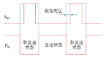
6.4 输入侧反并联开关管驱动存在死区
图19
为了避免此种安全隐患,需要在反并联开关管的驱动中添加死区,如图20所示,工程中可以根据实际使用的控制芯片通过软件或者硬件逻辑实现。但是,明显地,死区部分将会使得Z源逆变器工作于不正常工作状态,造成波形畸变。寻求一种可行的死区补偿方式或者新型的拓扑结构来解决这个矛盾应该是今后的研究思路。
图20
6.5 故障诊断技术空白
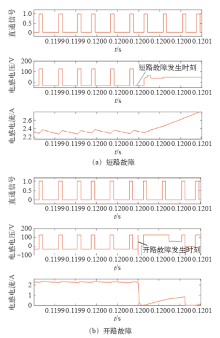
从逆变桥角度而言,由于允许直通,Z源逆变器相对于传统电压型逆变器具有更高的可靠性。但是对于其输入侧二极管而言,无论发生短路故障还是开路故障,都将给后级逆变桥带来不可逆转的损害。传统的DC-DC和DC-AC的故障诊断技术已经较为成熟,相关文献报道很多。就DC-DC而言,一般是以电感电流或电压状态来进行判断,故障发生时,电感电流上升/下降趋势和电感电压极性会与正常状态时相反[48,49,50,51]。而对于Z源逆变器来讲,正常工作时,在非直通状态下电感电压为负,电感电流呈下降趋势。发生短路故障时,电感电压为正,电感电流上升。发生开路故障时,电感电压有正有负,电感电流呈上升趋势,如图21所示,短路和开路故障分离困难。目前针对Z源逆变器的故障诊断及容错运行技术还未有会议或期刊文献报道,尚无切实有效的诊断方法。
图21
7 结论
相对于DC-DC变换器而言,Z源逆变器具有更高的可靠性,并且为单级结构,控制更为简单,具有其独特的吸引力。但是,Z源逆变器也具有其本身固有的缺陷,如升压比有限、功率体积比小,现在国内外的研究热点多集中于高升压比新拓扑、控制方法及多电平拓扑的研究,以光伏发电和电动汽车为应用背景的应用研究,取得了大量的成果。对Z源的缓冲电路设计、故障诊断和容错运行等方面少有研究,Z源逆变器的发展任重道远。
参考文献
Z-source inverter
[J].
DOI:10.1155/2014/539297
URL
PMID:25133241
[本文引用: 2]

In the conventional DC-AC inverter consisting of two DC-DC converters with unipolar output capacitors, the output capacitor voltages of the DC-DC converters must be higher than the DC input voltage. To overcome this weakness, this paper proposes a single-phase DC-AC inverter consisting of two embedded Z-source converters with bipolar output capacitors. The proposed inverter is composed of two embedded Z-source converters with a common DC source and output AC load. Though the output capacitor voltages of the converters are relatively low compared to those of a conventional inverter, an equivalent level of AC output voltages can be obtained. Moreover, by controlling the output capacitor voltages asymmetrically, the AC output voltage of the proposed inverter can be higher than the DC input voltage. To verify the validity of the proposed inverter, experiments were performed with a DC source voltage of 38 V. By controlling the output capacitor voltages of the converters symmetrically or asymmetrically, the proposed inverter can produce sinusoidal AC output voltages. The experiments show that efficiencies of up to 95% and 97% can be achieved with the proposed inverter using symmetric and asymmetric control, respectively.
Z-source inverter-based approach to the zero-crossing point detection of back EMF for sensorless brushless DC motor
[J].DOI:10.1109/TPEL.2014.2317708 URL [本文引用: 1]
An effective control method for quasi-Z-source cascade multilevel inverter-based grid-tie single-phase photovoltaic power system
[J].
DOI:10.1109/TII.2013.2280083
URL
[本文引用: 1]
An effective control method, including system-level control and pulsewidth modulation for quasi-Z-source cascade multilevel inverter (qZS-CMI) based grid-tie photovoltaic (PV) power system is proposed. The system-level control achieves the grid-tie current injection, independent maximum power point tracking (MPPT) for separate PV panels, and dc-link voltage balance for all quasi-Z-source H-bridge inverter (qZS-HBI) modules. The complete design process is disclosed. A multilevel space vector modulation (SVM) for the single-phase qZS-CMI is proposed to fulfill the synthetization of the step-like voltage waveforms. Simulation and experiment based on a seven-level prototype are carried out to validate the proposed methods.
An effective control method for three-phase quasi-Z-source cascaded multilevel inverter based grid-tie photovoltaic power system
[J].
DOI:10.1109/TIE.2014.2316256
URL
[本文引用: 1]
The quasi-Z-source cascaded multilevel inverter (qZS-CMI) presented many advantages over conventional CMI when applied in photovoltaic (PV) power systems. For example, qZS-CMI provides the balanced dc-link voltage and voltage boost ability, saves one-third modules, etc. However, current research studies only disclosed control of single-phase qZS-CMI-based PV power systems, and there was no literature related to control of three-phase qZS-CMI-based PV power systems. In this paper, for the first time, three-phase qZS-CMI's control is proposed and demonstrated for application to PV power systems. The models of PV-panel-fed qZS H-bridge module and qZS-CMI-based PV power system are built to accurately design control algorithms for each module and the whole system. The proposed control method includes the distributed maximum power point tracking for each module, dc-link peak voltage balance control for all modules, and grid-tie control for the whole system; moreover, a new multilevel space vector modulation method is proposed for the three-phase qZS-CMI. Simulation and experimental results on a test bench with a three-phase seven-level qZS-CMI-based PV power system verify the proposed control and modulation methods.
电动汽车双向阻抗源逆变器控制系统设计
[J].分析了双向功率流阻抗源逆变器系统工作原理、脉冲调制方式。采用开关信号流图方法建立了统一的控制系统模型,从稳态直流模型推导出系统额定工作点,从动态小信号模型推导出系统传递函数。阻抗源逆变器控制系统是含有二维参数的非线性系统,对相互关联的2个控制变量(直通占空比D和调制系数M)进行动态解耦,对解耦系统设计了电压电流双环控制器以提高系统的动态性能和稳定程度,基于伯德图分析了控制系统的稳定性和动态特性。研制了一台55 kVA双向功率流阻抗源逆变器,实验结果表明,系统具有优良性能,可以有效应用于电动汽车和可再生能源发电系统等领域。
Control system of bi-directional Z-source inverterfor electrical vehicles
[J].分析了双向功率流阻抗源逆变器系统工作原理、脉冲调制方式。采用开关信号流图方法建立了统一的控制系统模型,从稳态直流模型推导出系统额定工作点,从动态小信号模型推导出系统传递函数。阻抗源逆变器控制系统是含有二维参数的非线性系统,对相互关联的2个控制变量(直通占空比D和调制系数M)进行动态解耦,对解耦系统设计了电压电流双环控制器以提高系统的动态性能和稳定程度,基于伯德图分析了控制系统的稳定性和动态特性。研制了一台55 kVA双向功率流阻抗源逆变器,实验结果表明,系统具有优良性能,可以有效应用于电动汽车和可再生能源发电系统等领域。
Analysis and design of bi-directional Z-source inverter for electrical vehicles
[C].
Z源逆变器在提升电动汽车动力性能中的应用研究
[J].
Improvement of electric vehicle dynamic quality by Z-source inverter
[J].
Permanent-magnet synchronous motor drive system for electric vehicles using bidirectional Z-source inverter
[J].DOI:10.1049/iet-est.2011.0036 URL [本文引用: 1]
改善电动汽车动力性能的双向Z源逆变器控制策略
[J].
Control scheme of bi-directional Z-source inverter in improving the dynamic performance of electrical vehicles
[J].
Application of Z-source inverter for permanent-magnet synchronous motor drive system for electric vehicles
[C].
Z-源逆变器在光伏发电系统中的应用
[J].Z-源逆变器由于采用独特的X型Z-源网络,可以利用逆变器桥臂直通状态实现升压功能,从而使单级Z-源逆变器具有与两级并网系统相类似的性能。该文论述基于Z-源逆变器的光伏并网系统在变换效率、可靠性以及成本方面的优势,提出了一种新的单级Z-源逆变器并网系统两级控制策略, 该控制策略实现了MPPT控制和逆变器并网控制,使Z-源光伏并网系统能够动态跟踪光伏电池最大功率点电压,输出电流与电网电压同相位,从而达到较高的功率因数。软件仿真和实验分析证明了该控制方法具有优良的动、静态特性,适合各种变化的天气情况。
Study on Z-source inverter for photovoltaic generation system
[J].Z-源逆变器由于采用独特的X型Z-源网络,可以利用逆变器桥臂直通状态实现升压功能,从而使单级Z-源逆变器具有与两级并网系统相类似的性能。该文论述基于Z-源逆变器的光伏并网系统在变换效率、可靠性以及成本方面的优势,提出了一种新的单级Z-源逆变器并网系统两级控制策略, 该控制策略实现了MPPT控制和逆变器并网控制,使Z-源光伏并网系统能够动态跟踪光伏电池最大功率点电压,输出电流与电网电压同相位,从而达到较高的功率因数。软件仿真和实验分析证明了该控制方法具有优良的动、静态特性,适合各种变化的天气情况。
Impedance-source networks for electric power conversion Part I: a topological review
[J].DOI:10.1109/TPEL.2014.2313746 URL
Impedance-source networks for electric power conversion Part II: review of control and modulation techniques
[J].DOI:10.1109/TPEL.2014.2329859 URL
Lin ChienHui, et al. Development of an 85kW bidirectional quasi-Z-source inverter with DC-link feed-forward compensation for electric vehicle applications
[J].
DOI:10.1109/TPEL.2012.2237523
URL
[本文引用: 1]
This paper presents a detailed operation analysis, controller design, and realization of a high-power, bidirectional quasi-Z-source inverter (BQ-ZSI) for electric vehicle applications. The circuit analysis shows that with a bidirectional switch in the quasi-Z-source network, the performance of the inverter under small inductance and low power factor can be improved. Based on the circuit analysis, a small signal model of the BQ-ZSI is derived, which indicates that the circuit is prone to oscillate when there is disturbance on the dc input voltage. Therefore, a dedicated voltage controller with feed-forward compensation is designed to reject the disturbance and stabilize the dc-link voltage during a non-shoot-through state. An 85-kW prototype has been built. Both simulation and experimental results are presented to prove the functionality of the circuit and the effectiveness of the proposed control strategy.
A class of quasi-Z-source inverters
[C].
Improved Z-source inverter with reduced Z-source capacitor voltage stress and soft-start capability
[J].DOI:10.1109/TPEL.2008.2006173 URL [本文引用: 1]
串联型Z源光伏并网发电系统
[J].
Series Z-source grid-connected PV system
[J].
Trans-Z-source inverters
[C].
Γ-Z-source inverters
[J].
DOI:10.1109/TPEL.2013.2243755
URL
[本文引用: 1]
Voltage-type Gamma-Z-source inverters are proposed in this letter. They use a unique G-shaped impedance network for boosting their output voltage in addition to their usual voltage-buck behavior. Comparing them with other topologies, the proposed inverters use lesser components and a coupled transformer for producing the high-gain and modulation ratio simultaneously. The obtained gain can be tuned by varying the turns ratio gamma(Gamma Z) of the transformer within the narrow range of 1 < gamma(Gamma Z) <= 2. This leads to lesser winding turns at high gain, as compared to other related topologies. Experimental testing has already proven the validity of the proposed inverters.
New type T-source inverter
[C].
单相交流输入的无电解电容抽头电感单级升压逆变器在交流调速系统中的应用
[J].
DOI:10.13334/j.0258-8013.pcsee.2014.12.002
URL
[本文引用: 1]
研究将无电解电容的单级升压逆变技术应用于变频调速系统。采用的抽头电感单级升压逆变器(tapped- inductor single-stage boost inverter,TISSBI)包含由1个抽头电感和2个二极管构成的无源网络,通过调节直通占空比和电感抽头的位置,能够实现单级升降压功能。将无电解电容的TISSBI应用于单相输入的变频调速系统,实现抗电网电压跌落、母线脉动抑制和提高输入功率因数的功能。用实验验证了理论分析方法的可行性。
An adjustable speed system with single-phase AC input based on electrolytic capacitorless tapped-inductor single-stage boost inverters
[J].
DOI:10.13334/j.0258-8013.pcsee.2014.12.002
URL
[本文引用: 1]
研究将无电解电容的单级升压逆变技术应用于变频调速系统。采用的抽头电感单级升压逆变器(tapped- inductor single-stage boost inverter,TISSBI)包含由1个抽头电感和2个二极管构成的无源网络,通过调节直通占空比和电感抽头的位置,能够实现单级升降压功能。将无电解电容的TISSBI应用于单相输入的变频调速系统,实现抗电网电压跌落、母线脉动抑制和提高输入功率因数的功能。用实验验证了理论分析方法的可行性。
抽头电感单级升压逆变器的无源网络设计与参数极限值估计
[J].分析提出的抽头电感单级升压逆变器所有可能的运行状态,揭示在一个直通周期内,除了期望的3种运行状态外,还存在4种对能量传递过程不起作用,甚至给电路运行造成一定危害的运行状态。这4种运行状态可通过合理设计电感和电容值加以避免。从稳态分析中得到描述电路运行的状态方程组,展示能准确设计无源网络的方法,使其运行于期望的直通和非直通状态。提供的方法还可预测估计电感和电容的极限值,避免电路出现不正常的运行状态。仿真和实验验证了该设计方法的有效性和精确性,同时展示了当电感和电容低于极限值时出现的不正常运行状态。
Impedance network design and its critical value estimation of a tapped-inductor single-stage boost inverter
[J].分析提出的抽头电感单级升压逆变器所有可能的运行状态,揭示在一个直通周期内,除了期望的3种运行状态外,还存在4种对能量传递过程不起作用,甚至给电路运行造成一定危害的运行状态。这4种运行状态可通过合理设计电感和电容值加以避免。从稳态分析中得到描述电路运行的状态方程组,展示能准确设计无源网络的方法,使其运行于期望的直通和非直通状态。提供的方法还可预测估计电感和电容的极限值,避免电路出现不正常的运行状态。仿真和实验验证了该设计方法的有效性和精确性,同时展示了当电感和电容低于极限值时出现的不正常运行状态。
抽头电感准Z源逆变器
[J].提出一种高升压比的单级升压逆变器,它在传统准Z源逆变器拓扑中引入抽头电感无源网络,因此称为“抽头电感准Z源逆变器”(tapped inductor quasi-Z-source inverter,TL-qZSI)。该抽头电感无源网络包括一个抽头电感和两个二极管,替代了原准Z源逆变器中的一个电感。类似于抽头电感Z源逆变器(tapped inductor Z-source inverter,TL-ZSI),所提出的逆变器也能提供高升压能力,但比TL-ZSI略低些。分析电路的工作机理、升压能力和控制策略,讨论设计上的考虑。最后通过基于简单升压控制方法的实验结果验证该拓扑的实际性能。
Tapped inductor quasi-Z-source inverters
[J].提出一种高升压比的单级升压逆变器,它在传统准Z源逆变器拓扑中引入抽头电感无源网络,因此称为“抽头电感准Z源逆变器”(tapped inductor quasi-Z-source inverter,TL-qZSI)。该抽头电感无源网络包括一个抽头电感和两个二极管,替代了原准Z源逆变器中的一个电感。类似于抽头电感Z源逆变器(tapped inductor Z-source inverter,TL-ZSI),所提出的逆变器也能提供高升压能力,但比TL-ZSI略低些。分析电路的工作机理、升压能力和控制策略,讨论设计上的考虑。最后通过基于简单升压控制方法的实验结果验证该拓扑的实际性能。
耦合电感单级升压逆变器
[J].传统的两级式升压变换器通常由Boost变换器作为前级,以提升输入电压至合适的母线电压,防止输入电压较低时无法输出所需的交流电压。当升压比要求很高时,Boost变换器的占空比就会接近极限,过大的占空比会恶化Boost变换器的二极管反向恢复问题,增加开关管的开关损耗,降低效率。提出一种新型单级升压逆变器,在典型三相桥前加入包括耦合电感在内的无源网络,通过对耦合电感的设计和逆变桥直通时间的控制,可以使逆变器在直流输入电压较低时仍实现中间母线电压幅值的较大提升,输出稳定的交流电压。理论分析和实验结果表明该单级升压逆变器具有良好的性能。
A novel single-stage boost inverter with coupled inductors
[J].传统的两级式升压变换器通常由Boost变换器作为前级,以提升输入电压至合适的母线电压,防止输入电压较低时无法输出所需的交流电压。当升压比要求很高时,Boost变换器的占空比就会接近极限,过大的占空比会恶化Boost变换器的二极管反向恢复问题,增加开关管的开关损耗,降低效率。提出一种新型单级升压逆变器,在典型三相桥前加入包括耦合电感在内的无源网络,通过对耦合电感的设计和逆变桥直通时间的控制,可以使逆变器在直流输入电压较低时仍实现中间母线电压幅值的较大提升,输出稳定的交流电压。理论分析和实验结果表明该单级升压逆变器具有良好的性能。
L-Z-source inverter
[J].
DOI:10.1109/TPEL.2014.2303978
URL
[本文引用: 1]
On the basis of the classical Z-source inverter (ZSI), this paper presents a novel ZSI which only contains inductors and diodes in Z-source network. The inverter uses a unique inductor and diode network for boosting its output voltage, provides a common ground for the dc source and inverter, and avoids the disadvantage causing by capacitor in the classical ZSI and SL-ZSI, especially in prohibiting the inrush current at startup and the resonance of Z-source capacitors and inductors. The inverter can increase the boost factor through adjusting shoot-through duty ratio and increasing the number of inductor. The working principle of the proposed ZSI and comparison with the classical ZSI and SL-ZSI are analyzed in detail. Simulation and experimental results are given to demonstrate the operation features of the inverter.
Discussion and comments on L-Z source inverter
[J].DOI:10.1109/TPEL.2015.2421814 URL [本文引用: 1]
Extended boost active-switched-capacitor switched-inductor quasi-Z-source inverters
[J].DOI:10.1109/TPEL.2014.2379651 URL [本文引用: 1]
Switched-inductor quasi-Z-source inverter
[J].
DOI:10.1109/TPEL.2011.2141153
URL
[本文引用: 1]
This paper deals with a new family of high boost voltage inverters called switched-inductor quasi-Z-source inverters (SL-qZSIs). The proposed SL-qZSI is based on the well-known qZSI topology and adds only one inductor and three diodes. In comparison to the SL-ZSI, for the same input and output voltages, the proposed SL-qZSI provides continuous input current, a common ground with the dc source, reduced the passive component count, reduced voltage stress on capacitors, lower shoot-through current, and lower current stress on inductors and diodes. In addition, the proposed SL-qZSI can suppress inrush current at startup, which might destroy the devices. This paper presents the operating principles, analysis, and simulation results, and compares them with those of the SL-ZSI. To verify the performance of the proposed converter, a laboratory prototype was constructed with 48V(dc) input and an ac output line-to-line voltage of 120 V(rms). The simulation and experimental results verified that the converter has high step-up inversion ability.
Switched inductor Z-source inverter
[J].DOI:10.1109/TPEL.2010.2046676 URL [本文引用: 1]
A high set-up quasi-Z-source inverter based on voltage-lifting unit
[C].
Switched-coupled-inductor quasi-Z-source inverter
[J].
DOI:10.1021/acsami.9b19667
URL
PMID:31898449
[本文引用: 1]
Ultra-wide bandgap (UWBG) β-Ga2O3 is a promising material for next-generation power electronic devices. An enhancement-mode (E-mode) device is essential for designing power conversion systems with simplified circuitry and minimal loss. The integration of an E-mode FET with a depletion-mode (D-mode) FET can build a high-performance logic circuit. In this study, we first demonstrated the realization of an E-mode quasi-two-dimensional (quasi-2D) β-Ga2O3 FET with a novel graphene gate architecture via a van der Waals heterojunction. Then we monolithically integrated it with a D-mode quasi-2D β-Ga2O3FET, achieving an area-efficient logic circuit. The threshold voltage of the n-channel UWBG β-Ga2O3 material was controlled by forming a novel architecture of double-gate graphene/β-Ga2O3 heterojunction, where both graphene and β-Ga2O3 were obtained by a mechanical exfoliation method. The fabricated double graphene-gate β-Ga2O3 MESFET was operated in E-mode with a positive threshold voltage of +0.25 V, which is approximately 1.2 V higher than that of a single-gate D-mode β-Ga2O3 MESFET. Both E-/D-modes β-Ga2O3 MESFETs showed excellent electrical characteristics with a subthreshold swing of 68.9 and 84.6 mV/dec, respectively, and a high on/off current ratio of approximately 107. A β-Ga2O3 logic inverter composed of E-/D-mode β-Ga2O3 devices exhibited desired inversion characteristics. The monolithic integration of a E-/D-mode quasi-2D FET with an UWBG channel layer can pave the way for various applications in smart and robust power (nano)electronics.
An energy-stored quasi-Z-source inverter for application to photovoltaic power system
[J].
DOI:10.1109/TIE.2012.2217711
URL
[本文引用: 1]
The quasi-Z-source inverter (qZSI) with battery operation can balance the stochastic fluctuations of photovoltaic (PV) power injected to the grid/load, but its existing topology has a power limitation due to the wide range of discontinuous conduction mode during battery discharge. This paper proposes a new topology of the energy-stored qZSI to overcome this disadvantage. The operating characteristic of the proposed solution is analyzed in detail and compared to that of the existing topology. Two strategies are proposed with the related design principles to control the new energy-stored qZSI when applied to the PV power system. They can control the inverter output power, track the PV panel's maximum power point, and manage the battery power, simultaneously. The voltage boost and inversion, and energy storage are integrated in a single-stage inverter. An experimental prototype is built to test the proposed circuit and the two discussed control methods. The obtained results verify the theoretical analysis and prove the effectiveness of the proposed control of the inverter's input and output powers and battery power regardless of the charging or discharging situation. A real PV panel is used in the grid-tie test of the proposed energy-stored qZSI, which demonstrates three operational modes suitable for application in the PV power system.
Z-source inverter for motor drives
[J].DOI:10.1109/TPEL.2005.850938 URL [本文引用: 1]
A novel quasi-Z-source inverter topology with special coupled inductors for input current ripples cancellation
[J].DOI:10.1109/TPEL.2014.2343012 URL [本文引用: 1]
Maximum boost control of the Z-source inverter
[J].DOI:10.1109/TPEL.2005.850927 URL [本文引用: 1]
Maximum constant boost control of the Z-source inverter
[C].
Pulse-width modulation of Z-source inverters
[J].DOI:10.1109/TPEL.2005.857543 URL [本文引用: 2]
Current ripple comparison between ZSVM4 and ZSVM2
[J].
DOI:10.15420/aer.2017.20.1
URL
PMID:29018519
[本文引用: 1]
Recurrent episodes of ventricular tachycardia in patients with structural heart disease are associated with increased mortality and morbidity, despite the life-saving benefits of implantable cardiac defibrillators. Reducing implantable cardiac defibrillator therapies is important, as recurrent shocks can cause increased myocardial damage and stunning, despite the conversion of ventricular tachycardia/ventricular fibrillation. Catheter ablation has emerged as a potential therapeutic option either for primary or secondary prevention of these arrhythmias, particularly in post-myocardial infarction cases where the substrate is well defined. However, the outcomes of catheter ablation of ventricular tachycardia in structural heart disease remain unsatisfactory in comparison with other electrophysiological procedures. The disappointing efficacy of ventricular tachycardia ablation in structural heart disease is multifactorial. In this review, we discuss the issues surrounding this and examine the limitations of current mapping approaches, as well as newer technologies that might help address them.
Pulsewidth modulation of Z-source inverters with minimum inductor current ripple
[J].
DOI:10.1109/TIE.2013.2240632
URL
[本文引用: 1]
This paper proposes the pulsewidth modulation (PWM) strategy of Z-source inverters (ZSIs) with minimum inductor current ripple. In existing PWM strategy with single-phase shoot-through, the shoot-through time interval is divided into six equal parts, therefore the three phase legs bear the equal shoot-through time interval. In this manner, the allotment and arrangement of the shoot-through state is easy to realize, but the inductor current ripple is not optimized. This causes to use relatively large inductors. In the proposed PWM strategy, the shoot-through time intervals of three phase legs are calculated and rearranged according to the active state and zero state time intervals to achieve the minimum current ripple across the Z-source inductor, while maintaining the same total shoot-through time interval. The principle of the proposed PWM strategy is analyzed in detail, and the comparison of current ripple under the traditional and proposed PWM strategy is given. Simulation and experimental results on the series ZSI are shown to verify the analysis.
Optimal design of the inductor in Z-source inverter with single phase shoot-through SVPWM strategy
[C].
A direct peak DC-link boost voltage control strategy in Z-source inverter
[C].
A direct DC-link boost voltage PID-like fuzzy control strategy in Z-source inverter
[C].
Voltage and current-programmed modes in control of the Z-source converter
[J].DOI:10.1109/TIA.2010.2040054 URL [本文引用: 1]
Design and development of a 50kW Z-source inverter for fuel cell vehicles
[C].
Analysis and design of snubber circuit for Z-source inverter
[C].
Operation modes and characteristics of the Z-source inverter with small inductance or low power factor
[J].
DOI:10.3174/ajnr.A6343
URL
PMID:31896567
[本文引用: 1]
Vascular devices generating high shear stress can cause type 2A acquired von Willebrand disease, which is characterized by low von Willebrand factor activity accompanied by hemorrhagic complications. The braided mesh structure of flow-diverting stents with a relatively small strut size can create abnormally high shear stress while arterial blood flows through the stent struts into the aneurysm, and flow-diverting stent may be associated with reduced von Willebrand factor activity.
适应负载大范围变动的高性能Z-源逆变器
[J].
Fuzzy PID controller for DC-link boost volt-age in Z-source inverter
[J].
Open- and short-circuit switch fault diagnosis for nonisolated DC-DC converters using field programmable gate array
[J].
DOI:10.1109/TIE.2012.2224078
URL
[本文引用: 1]
Fault detection (FD) in power electronic converters is necessary in embedded and safety critical applications to prevent further damage. Fast FD is a mandatory step in order to make a suitable response to a fault in one of the semiconductor devices. The aim of this study is to present a fast yet robust method for fault diagnosis in nonisolated dc-dc converters. FD is based on time and current criteria which observe the slope of the inductor current over the time. It is realized by using a hybrid structure via coordinated operation of two FD subsystems that work in parallel. No additional sensors, which increase system cost and reduce reliability, are required for this detection method. For validation, computer simulations are first carried out. The proposed detection scheme is validated on a boost converter. Effects of input disturbances and the closed-loop control are also considered. In the experimental setup, a field programmable gate array digital target is used for the implementation of the proposed method, to perform a very fast switch FD. Results show that, with the presented method, FD is robust and can be done in a few microseconds.
Fault diagnosis of PWM DC-DC converters based on magnetic component voltages equation
[J].
DOI:10.1109/TPEL.2013.2283881
URL
[本文引用: 1]
Switch fault diagnosis is an important design aspect for pulse width modulation (PWM) dc-dc power converters. It can prevent power converters from further damage, and also make preparations for remedial actions. In this paper, a fast switch fault diagnostic method is proposed for PWM dc-dc converters operating in continuous conduction mode. The proposed method utilizes the magnetic component (inductor or transformer) voltage for fault diagnosis. Based on the real-time voltage measurement and switch gate-driver signals, characteristics of switch open-circuit faults and short-circuit faults are rapidly extracted, and thus, switch faults can be quickly detected. The magnetic component voltage can be measured by an auxiliary winding in the magnetic core, and gate-driver signals can be easily got from the control circuit. Moreover, the fault detection can be implemented by a low-cost logical hardware circuit, and this circuit can be integrated into the control circuit. The fault diagnosis principle, design considerations, and implementation are discussed in this paper. Experiments are conducted to verify the theoretical analysis.
Photovoltaic systems reliability improvement by real-time FPGA-based switch failure diagnosis and fault-tolerant DC-DC converter
[J].
Single-switch DC-DC converter with fault-tolerant capability under open- and short-circuit switch failures
[J].DOI:10.1109/TPEL.2014.2342878 URL [本文引用: 1]
