

1 引言
EPS应急电源是为满足消防需要而设计的电源,在现代高层建筑中广泛应用。EPS应急电源充电机部分采用PWM可控整流装置可实现网侧电流正弦化,功率因数可控,直流输出电压、电流可调;同时,降低了充电机对电网的谐波污染,提高了系统的功率因数,降低了无功损耗。
鉴此,本文设计实现了基于ALTER公司 Cyclone Ⅲ Ep3c25E144C8n FPGA控制芯片的应急电源充电装置,实现对蓄电池的安全高效充电。
2 可控整流装置拓扑结构及控制策略分析
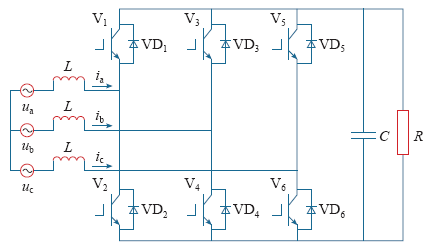
文中的三相PWM可控整流装置采用三相电压型半桥整流电路,主要由网侧电感、整流桥和直流侧电容等组成,其拓扑结构如图1所示。网侧电感实现电流谐波的抑制,使网侧电流正弦化运行。直流侧利用电容作为储能元件,提高直流电压的抗干扰性能和直流电压的快速跟随能力。
图1
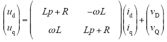
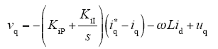
由式(1)可看出,有功电流id与无功电流iq相互耦合,无法实现对有功分量和无功分量的独立调节。为此采用前馈解耦的控制策略,实现控制器设计。设在两相旋转(d,q)坐标系下d轴电压vd与电网电压峰值Um相等,即Vd=Um,q轴分量Vq=0。设置vq和vd的解耦控制方程为
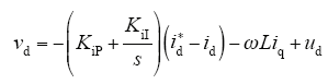
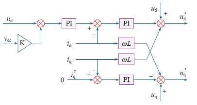
由式(2)、式(3)可见,通过解耦可实现有功电流和无功电流的独立控制,系统的控制框图如图2所示。
图2
3 整流装置建模及仿真实验
3.1 整流装置建模
图3
仿真模型的参数如下:电网输入电压160V、50Hz,网侧电感4mH,直流侧电容1 400μF,电压外环Kp = 0.053,Ki = 0.4,电流内环Kp = 0.8,Ki = 1.3。
3.2 仿真实验
图4
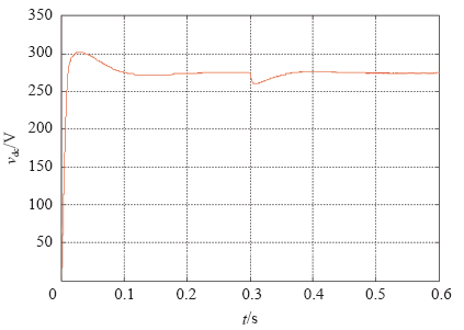
图5
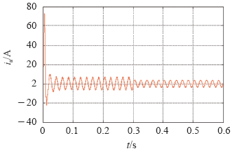
图6
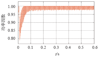
图5为负载改变时,网侧A相电流的仿真输出波形。 负载为50Ω时,输出电压274V,输出功率为1 500W,网侧输出电流为5.4A,当负载改变为100Ω时,输出功率减半,网侧电流减小为2.7A。
图6为负载改变时,网侧A相电流的仿真输出波形,稳定运行状态下,系统的功率因数大于0.97,基本处于单位功率因数整流运行状态。
4 实验样机设计及结果分析
4.1 实验样机设计
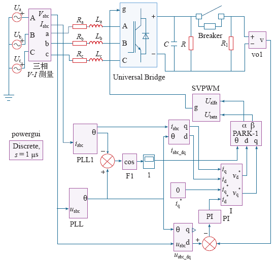
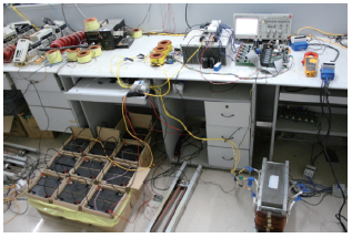
本文设计了1 500W基于FPGA CycloneⅢ Ep3c25E144C8n芯片控制的三相电压型PWM整流装置,为EPS应急电源蓄电池组(12V/17Ah/20节串联)充电。该系统硬件电路包含:主电路、控制电路、开关管驱动电路和信号采样电路。软件采用VHDL语言设计,主要包括:鉴相模块,AD采样模块,滤波模块和PWM波形产生模块等。样机框图如图7所示。
图7
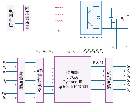
图7
三相PWM整流装置硬件结构图
Fig.7
The hardware structure diagram of three-phase PWM rectifier
借鉴上面的仿真结果,经反复实验,样机参数选择如下:电网输入电压380V、50Hz,降压变压器电压比380/160,开关频率12.8kHz,网侧电感8mH,直流侧电容940μF,电压外环Kp = 1,Ki = 100,电流内环Kp = 0.01,Ki = 5。
4.2 实验结果分析
4.2.1 阻性负载实验
图8
图9
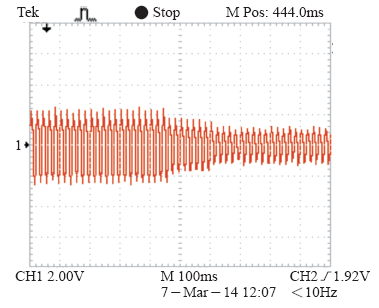
图10
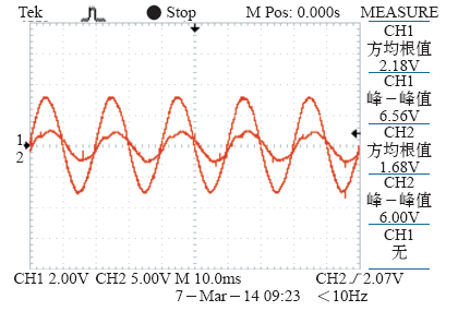
图9为负载改变时,网侧A相电流的实验输出波形,此波形为采样输出波形,负载发生改变时,电流幅值减小,电流基本处于正弦化运行状态。
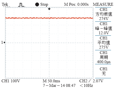
图10为50Ω负载稳定运行状态A相电压和电流的采样信号波形,由于采样信号为AB线电压和A相电流波形,理论上电压超前30°,因此实验样机稳定运行状态时功率因数基本为1。
4.2.2 蓄电池负载实验
图11
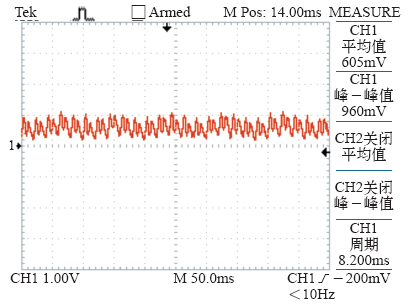
图12
图13
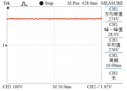
图14
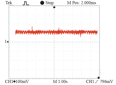
图15
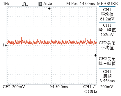
图16
5 结论
本文设计了基于FPGA的三相应急电源充电装置。仿真实验结果显示,输出的直流电压稳定,电压波动在5V以内,负载改变时抗干扰性能强;网侧电流正弦度良好,电流谐波小;稳定运行时功率因数大于0.97。样机实验结果证明变载状态下直流电压、网侧电流能快速恢复到稳定状态,系统具有良好的鲁棒性,且基本运行在单位功率因数状态下。采用分级定流的充电方式可在10h内安全地完成充电,满足应急电源充电标准,实验样机可应用到实际工程中。
附 录
附图
参考文献
基于FPGA的精跟踪系统
[J].
Fine tracking system based on FPGA
[J].
基于FPGA的高速数据采集系统设计
[J].
Design and development of the high-speed data acquisition system based on FPGA
[J].
FPGA器件设计技术发展综述
[J].
DOI:10.3724/SP.J.1146.2009.00751
URL
PMID:31882987
[本文引用: 1]

In the present study, we aim to help improve the design of van der Waals stacking, i.e., vertical 2D electronics, by probing charge transport differences in both parallel and vertical conducting channels of layered molybdenum disulfide (MoS2), with thin graphite acting as source and drain electrodes. To avoid systematic errors and variable contact contributions to the MoS2 channel, parallel and vertical electronics are all fabricated and measured on the same conducting material. Large differences in the on/off current ratio, mobility, and charge fluctuations, between parallel and vertical electronics are evident in electrical performance as well as in charge transport mechanisms. Further insights are drawn from a well-constrained analysis of both temperature-dependent current-voltage characteristics and low-frequency (LF) current fluctuations. This work offers significant insight into the fundamental understanding of charge transport and the development of future layered-materials-based integration technology.
An overview to FPGA device design technologies
[J].
DOI:10.3724/SP.J.1146.2009.00751
URL
PMID:31882987
[本文引用: 1]
In the present study, we aim to help improve the design of van der Waals stacking, i.e., vertical 2D electronics, by probing charge transport differences in both parallel and vertical conducting channels of layered molybdenum disulfide (MoS2), with thin graphite acting as source and drain electrodes. To avoid systematic errors and variable contact contributions to the MoS2 channel, parallel and vertical electronics are all fabricated and measured on the same conducting material. Large differences in the on/off current ratio, mobility, and charge fluctuations, between parallel and vertical electronics are evident in electrical performance as well as in charge transport mechanisms. Further insights are drawn from a well-constrained analysis of both temperature-dependent current-voltage characteristics and low-frequency (LF) current fluctuations. This work offers significant insight into the fundamental understanding of charge transport and the development of future layered-materials-based integration technology.
基于电源电流和负载电流检测的前馈加反馈的三相四线制APF控制策略
[J].
Feedforward-feedback control strategy based on detection of power current and load current for three-phase four-wire APF
[J].
三相电压型PWM整流的新型双闭环控制策略
[J].同步旋转d-q坐标系下的电压、电流双闭环控制,广泛应用于三相电压型PWM整流器。该方案结构简单,比较适合基于数字处理芯片的数字控制系统。由于交流侧电感工艺存在差异,且当电流很大电感饱和时,电感值也会有变化,实际控制系统往往忽略掉耦合项;而电压外环的非线性也使得控制系统的性能提升受到限制。提出一种新的电压电流双闭环控制策略,其中电流内环借鉴合成矢量的思想,提出同步旋转d-q坐标系下无电感L参数的电流解耦控制方法;电压外环采用电压平方为控制量实现线性化的间接电压控制。仿真与实验结果均验证了所提方法的正确性和有效性。
A novel double closed loops control of the three-phase voltage-sourced pwm rectifier
[J].同步旋转d-q坐标系下的电压、电流双闭环控制,广泛应用于三相电压型PWM整流器。该方案结构简单,比较适合基于数字处理芯片的数字控制系统。由于交流侧电感工艺存在差异,且当电流很大电感饱和时,电感值也会有变化,实际控制系统往往忽略掉耦合项;而电压外环的非线性也使得控制系统的性能提升受到限制。提出一种新的电压电流双闭环控制策略,其中电流内环借鉴合成矢量的思想,提出同步旋转d-q坐标系下无电感L参数的电流解耦控制方法;电压外环采用电压平方为控制量实现线性化的间接电压控制。仿真与实验结果均验证了所提方法的正确性和有效性。
基于三闭环控制的PWM整流充电技术的研究
[J].
Research on PWM rectifier and charging technique based on three closed-loop controlling
[J].
空间矢量PWM整流器仿真研究
[J].
The Investigation on the PWM rectifier using the SVPWM
[J].
双闭环矢量控制的电压型PWM整流器参数整定
[J].The PI parameter setting of double closed-loop vector control of voltage source PWM rectifier is very important and largely depending on experience with few references available. In this paper, how the L、C values and PI parameters influence the output DC voltage waveform, AC side harmonics and power factor are studied by simulation in Matlab/Simulink, and based on which a simple and normalized method for the control system design and PI parameter setting is proposed. Some examples are given to illustrate the application of this method.
Parameter setting for double closed-loop vector control of voltage source PWM rectifier
[J].The PI parameter setting of double closed-loop vector control of voltage source PWM rectifier is very important and largely depending on experience with few references available. In this paper, how the L、C values and PI parameters influence the output DC voltage waveform, AC side harmonics and power factor are studied by simulation in Matlab/Simulink, and based on which a simple and normalized method for the control system design and PI parameter setting is proposed. Some examples are given to illustrate the application of this method.
基于可逆PWM整流器的蓄电池充放电装置
[J].
Battery charge and discharge device based on reversible PWM rectifier
[J].
