


1 Introduction
In 2002, Z-source inverter (ZSI) was firstly introduced to power electronics area as a new voltage-fed topology and has been proven experimentally[1]. Z-source inverters have several advantages and disadvantages, which have been extensively reviewed in Ref.[2-4]. The key notion of ZSI is established by using a diode in the front end, and two inductors and two capacitors connected in the X-shaped. In 2008, Professor F. Z. Peng proposed the improved version of ZSI, that is, quasi-Z-source inverter (qZSI)[5]. Along with the advantages of ZSI, qZSI has several merits of their own, such as reduced passive component ratings, continuous input current, a common dc rail between the source and inverter, etc[6]. Many topologies have been derived from the primary Z-source power converter, such as Z/quasi-Z-source AC-AC converter, Z/quasi-Z-source DC-DC converter, Y-source converter, X-source converter, etc. From then on, quasi-Z-source inverter has been widely applied in lots of areas such as electric vehicle, photovoltaic generation, wind power generation, etc.
The conventional bidirectional DC-DC power converters, such as bidirectional Buck-Boost power converter and Cuk bidirectional DC-DC power converter are introduced in Ref.[6-7]. In the bidirectional Buck-Boost converter, it can invert the polarity of the voltage, and can either increase or decrease the voltage magnitude. But it is only applicable to small and medium-sized power applications. As for the Cuk bidirectional DC-DC power converter, one of its principal advantages over conventional converters is that both the input and output currents are nonpulsating, but due to the complicated circuit, the efficiency of the power convertion is not high enough. However, with the development of science and technology, quasi-Z-source inverter has been proposed. It inherits all the advantages of the traditional ZSI and has several more advantages, including reduced passive component stress and continuous input current features[8,9,10,11]. These advantages make it easier to be applied in bidirectional power converters.
In this manuscript, a DC-DC circuit based on the existing quasi-Z-source converter topology is proposed. This proposed circuit topology contains all the benefits of existing quasi-Z-source-based power converters, such as buck-boost function of the single topological structure, reversal of the polarity of the input/output voltage and high reliability owing to their immunity from shoot-through and open-circuit problems. In addition to that, the proposed circuit topology can be applied to DC-DC power conversion which has more freedom for increasing voltage gain by regulating the duty cycle D. So, it can be widely used in a variety of electric power supply systems, including cars, ships, aircraft, computers, even in the microgrid.
This paper focuses on the construction of DC-DC power converter topology based on quasi-Z-source. The rest of this manuscript is structured as follows. In Section 2, the operating principle and equivalent circuits are introduced and verified. Then, the results of simulation and experiments are shown in Section 3, followed by the conclusion in Section 4.
2 Proposed Circuit Topology
2.1 Circuit topology
The circuit topology of a quasi-Z-source-based DC-DC converter is shown in Fig.1. Apparently, its main circuit is similar to the quasi-Z-source-based converter, where two capacitors C1、C2 and two inductors L1、L2 are used. As for the power switches, two IGBT modules or power MOSFETs are face-to-face connected, each of them is conventionally composed of a power transistor and an anti-paralleled diode, and this will be convenient to use the existing IGBT module or power MOSFET. Due to the power switches, the circuit can transmit bi-directional power flow.
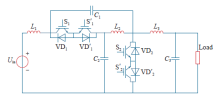
Fig.1
Circuit configuration of the proposed DC-DC power converter
Same to the conventional Z-source converters, the quasi-Z-source-based converter has a symmetrical network in which C1 = C2, L1 = L2. The switches S1 and S2 are considered as a pair of complementary working switches. Apparently, the diode 


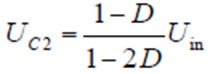
(1) When the power flow is transmitted from the left side to the right side, the equivalent circuit is shown in Fig.2. There are two operating modes in this case, one is the switch S1 is on and switch S2 is off, and the other is switch S1 is off and switch S2 is on. In the former case, the inductors L1、L2 and L3 are charged, the capacitors C1 and C2 are discharged, the equivalent circuit is shown in Fig.2a.
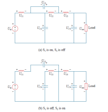
Fig.2
Equivalent circuit of the forward power flow
From the equivalent circuit diagram, Fig.2a, one has

Where Uin is the input dc voltage and Uout is the output dc voltage.
In the latter case, that is, when the switch S2 is on and the switch S1 is off. In this case, the inductors L1、L2 and L3 are discharged, the capacitors C1 and C2 are charged, the equivalent circuit is shown in Fig.2b.
From the equivalent circuit diagram, Fig.2b, one has

At steady state, the average voltage of the inductors over one switching period should be zero. Hence, from Equ. (1) and Equ. (2), we have
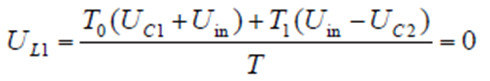
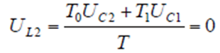
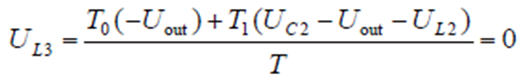
Where T0 is the duration of S1 at the on state and T1 is the duration of it at the off state.
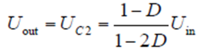
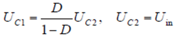
From Equ. (3)~(5), the voltage of the capacitors C1 and C2 can be expressed as
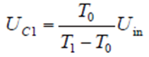
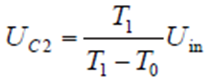
Hence, we have
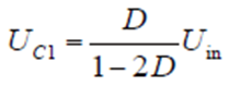
Where D is the duty cycle of the switch S2.
(2) When the power flow is transmitted from the right side to the left side, the equivalent circuit is shown in Fig.3. The power switches 


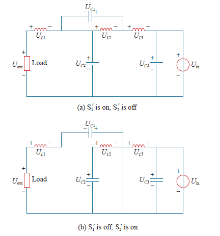
Fig.3
Equivalent circuit of the reverse power flow
From the above discussion in (1), we can have the similar conclusion
Where D is the duty cycle of the switch 
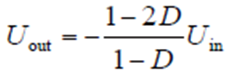
2.2 Voltage gain G versus duty cycle D
The plot of voltage gain G versus duty cycle D is shown in Fig.4, which makes it clear that the relationship between voltage and duty cycle D. In this figure, the case is when the power flow is transmitted from the left side to the right side. When D varies from 0 to 0.5, the output voltage is with the input voltage polarity, the circuit operates in boost mode; when D varies from 0.5 to 1, the polarity of output voltage and input voltage are reversal. Wherein, when D varies from 0.5 to 0.667, the circuit operates at reverse boost mode; when D varies from 0.667 to 1, it operates at reverse buck mode. From the above analysis, it is quite clearly that the output voltage can be adjusted by adjusting the duty cycle D of switch S2( 
Fig.4
Relationship diagram of voltage gain versus duty cycle
3 Simulation and Experimental Results
The simulation is performed using the software Saber. A prototype for the proposed DC-DC power converter is fabricated. The simulation diagram of the proposed DC-DC power converter is shown in Fig.5 and the simulation results are shown in Fig.6. System parameters for simulation are given as follows:
(1) DC input voltage Uin = 24V.
(2) Inductors and capacitors of the quasi-Z-source: L1 = L2 = L3 = 1mH, C1 = C2 = C3 = 500µF.
(3) System switching frequency f = 20kHz.
(4) The load resistor value R = 10Ω.
When the quasi-Z-source-based converter is applied to DC-DC power conversion, and the power flow is transmitted from the left side to the right side, the simulation results are shown in Fig.6a. Setting the input voltage on 24V, and adjusting the duty cycle of switch S2 to 0.2. According to Equ. (10), the theoretical value of output voltage is 32V. It can be seen from the simulation waveform in Fig.6a that the output voltage is 32.038V. The voltage of capacitor C1 is 7.954 5V, which theoretical value is 8V; The voltage of capacitor C2 is 31.967V, which theoretical value is 32V; The currents of the inductors are all flat, which verify the accuracy of the above theoretical analysis. It is clearly that the simulation results are nearly perfect to verify the conclusion in Section 2.
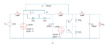
Fig.5
Simulation diagram of the proposed DC-DC power converter
When the power flow is transmitted from the right side to the left side, the simulation results are shown in Fig.6b. The input voltage is also 24V, and the duty cycle of switch S2 is still 0.2. According to Equ. (12), the theoretical value is 18V. It can be seen from the simulation waveform in Fig.6b that output voltage is 18.002V. The voltage of capacitor C1 is 6.003 4V, which theoretical value is 6V; The voltage of capacitor C2 is 23.997V, which theoretical value is 24V; The currents of the inductors are also flat, which could also verify the accuracy of the above theoretical analysis.
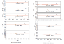
Fig.6
Simulation waveforms of the bidirectional power flow
Finally, from the above simulation results, it can be seen that when the power flow is transmitted from the left side to the right side, the quasi-Z-source-based converter can achieve boost function and maintain output voltage stability. On the other hand, when the power flow is transmitted from the right side to the left side, the quasi-Z-source-based converter can achieve buck function. All these waveforms was confirmed that the proposed circuit operated following the theory, which can indeed transmit bidirectional power flow in a single topology with a good accuracy by regulating the duty cycle D.
The prototype has been constructed in lab that is shown in Fig.7. The same parameters are used in the experimental work which is shown in the above section. DSP TMS320F2812 is used as a tool for generating signals to control the switches. It has all necessary circuits, which includes PWM generator; This DSP chip can generates four routes of signals, which can be divided into two groups to control S1、S2 and switches 


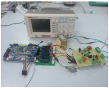
Fig.7
Experimental circuit prototype
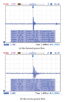
Fig.8
Experimental results of the proposed DC-DC power conversion when D = 0.2
As can be seen in Fig.8, when the power flow is transmitted from the left side to the right side, the quasi-Z-source-based DC-DC converter can boost the voltage from 24V to the average voltage 32.2V; When the power flow is transmitted from the right side to the left side, the quasi-Z-source-based DC-DC converter can buck the voltage from 24V to the average voltage 18.1V. All of these experimental results are in good agreement with the previous analysis. The peak voltage of the output voltage waveform was caused by several aspects including EMI, existence of nonlinear components and switches instant action. It can be restricted by adding the embedded absorption circuit on the switches.
The simulation and experimental results validate the advantages of the proposed quasi-Z-source-based DC-DC power converter topology. It can either boost or buck the voltage in a single topology, and the output voltage is stable with high accuracy and a small ripple.
4 Conclusion
This paper has presented a comprehensive study on the DC-DC power converter topology based on quasi-Z-source concept. Both simulation and experiments confirmed that the proposed DC-DC power converter topology can transmit bidirectional power flow in a single topology by PWM control. It can also extend the regulating range to more than that can be achieved in the conventional DC-DC converters. The circuit can not only provide buck-boost function, but also reverse polarity of the input/output voltage. Due to the uniqueness of this circuit structure, it can increase efficiency and reliability, overcome the conceptual and theoretical barriers and limitations of the conventional power converters and provide a novel all-purpose power converter topology. With these merits, it can broad the application of power converters based on Z-source/quasi-Z-source.
This paper describes the operating principle, analyzes the circuit characteristics, the simulation and experimental results, which presented to verify the rationality and superiority of the circuit topology. Due to the page limit, the simulation and experimental results will be provided in the future papers to demonstrate the features of the AC-AC power converter topology based on quasi-Z-source in the same topology.
参考文献
Comparison of traditional inverters and Z-source inverter for fuel cell vehicles
[J].
Comparison of three phase three-level Z-source inverter and quasi-Z-source inverter characteristics
[C].
Comparison of three-phase three-level DC-DC boosted inverters
[J].
Four quasi-Z-source inverters
[C].
Dynamic analysis of switching-mode DC/DC converters
[M].
Topologies of bidirectional PWM dc-dc power converters
[C].
CCM and DCM operation analysis of cascaded quasi-Z-source inverter
[C].
Switched inductor Z-source inverter
[J].
Trans-Z-source inverters
[J].
Z-source DC-DC converter with cascade switched capacitor
[C].
A family of Z-source and quasi-Z-source dc-dc converters
[C].
Modifcation of quasi-Z-source inverter operating in stand-alone power system
[C].
CCM and DCM operation analysis of cascaded quasi-Z-source inverter
[C].
Quasi-Z-source-based isolated DC/DC converters for distributed power generation
[J].
Dc-to-dc converters with continuous input and output power
[J].
Hybrid-source networks: Layouts and generalized cascading concepts
[J].
Bidirectional cascaded quasi-Z-source DC-DC converter
[C].
High-voltage boost quasi-Z-source isolated DC/DC converter
[J].
Design and digital implementation of voltage and current mode control for the quasi-Z-source converters
[J].
High efficiency isolated Boost DC-DC converter for high-power low-voltage fuel cell applications
[J].
Modeling and control of quasi-Z-source inverter for distributed generation applications
[J].
