


1 引言
文献[5]将Boost变换器的电感与反激变换器的初级侧集成于同一磁心,提出一种新型升压变换器,集成升压–反激变换器(Integrated Boost-Flyback step-up Converter,IBFC)。IBFC具有如下优势:在较小占空比条件下增加了升压增益范围,达到较高工作效率;可降低输入端电流谐波,改善电路功率因数;反激变换器漏感可实现有源元件的零电压或零电流关断,减少了器件的电压应力[7,8,9,10]。但随着升压倍数的不断提高,为避免占空比过大,必须增加反激变换器的匝数比,将导致变压器漏感比例过大,引起严重的开关管关断电压尖峰。其次,会造成输出电压在输出电容间的不平均分配,增大电容与二极管的电压应力。此外,反激变换器一次侧易产生较高电流增益,增加开关管的电流应力,造成不必要的损耗,限制了IBFC的应用场合[11]。
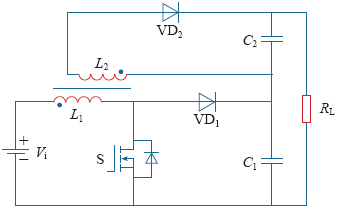
图1
为解决上述电路存在的缺陷,将IBFC中Boost电路替换为耦合电感升压电路,构成本文提出的集成耦合电感升压–反激变换器(Integrated Coupled-inductor Boost-Flyback Converter,ICBFC)。该变换器利用耦合电感及反激变换器共同升压,具有显著的优点:有效抑制二极管反向恢复电流,降低反向恢复损耗;降低开关管电流应力,减小开关损耗;减少输出电压的纹波并使电路保持较高功率密度。
文章共分三部分:首先提出ICBFC电路,分析了其工作模式。其次,通过状态空间平均法研究了ICBFC内部各变量与寄生参数间的关系,建立了电流连续工作模式(CCM)下的小信号模型,设计出相应的闭环控制系统。最后通过仿真与实验验证了建模和闭环控制器的正确性和可行性。
2 集成耦合电感升压–反激变换器稳态工作原理及小信号建模
2.1 稳态工作原理分析
图2
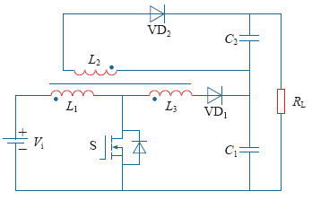
图3
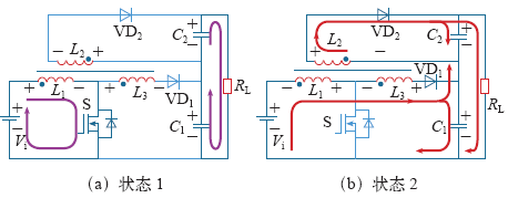
图3
集成耦合电感升压- 反激变换器稳态工作原理
Fig.3
Equivalent circuit of integrated coupled inductor Boost-flyback converter in steady state
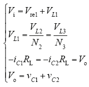
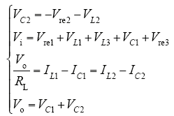
设开关管在一个工作周期内导通时间为t1,关断时间为t2,反激变压器一、二次侧绕组匝数比为1∶N2,耦合电感L1、L3匝数比为1∶N3,电路工作状态有两个:
状态1:如图3a所示,开关管S导通时,电源为反激变压器一次侧充电,形成回路Vi-L1-S。反激变压器二次侧电感的感应电动势与L1电位相反,耦合电感与L1电位相同,二极管VD1、VD2反向偏置,反激变压器及耦合电感处于储能阶段,在t1时段末电感电流充电达到峰值,与此同时,输出电容C1、C2给负载RL提供能量。
状态2:如图3b所示,开关管S关断,反激变压器一、二次侧感应电动势方向与状态1反向,二极管VD1、VD2导通,电源和电感L1、L3共同为电容C1充电形成回路Vi-L1-L3-VD1-C1,同时二次侧电感L2给电容C2充电,形成回路L2-VD2-C2。电感为电容充电的同时也为负载提供能量,由于反激变压器及耦合电感同时为输出电容及电路负载提供能量,因此t2阶段流过电感L1、L2、L3的电流值逐渐减少,在t2时段末电感电流达到最小值。
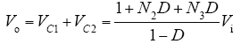
通过对以上状态的分析,在CCM模式下,根据电感伏秒平衡求出输入、输出端电压关系
2.2 小信号模型的建立
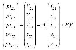
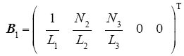
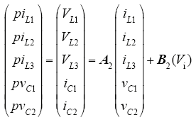
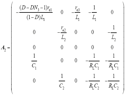
在该变换器中,反激变压器及耦合电感作为主要储能元件在整个电路工作过程中起到重要作用,电感L1、L2、L3的寄生电阻对电路内部电压及电流变化产生很大影响,因此在模型建立过程中加入反激变压器一、二次侧电感及耦合电感寄生电阻re1、re2、re3。设与系统中储能元件对应的电感电流iL1、iL2、iL3,电容电压vC1、vC2为系统状态变量,输入电压Vi及电路占空比D作为系统的输入信号。
采用状态空间平均法对该变换器建模,其状态平均方程如下
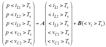
式中,p为微分算子,p = d/dt。
模式1:当开关管导通时,电源为电感L1充电,电容C1、C2为负载RL供电,由式(3)和式(4)可列出模式1下电路的状态空间方程
其中
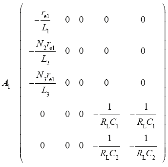
模式2:开关管关断时,电源和电感L1、L3共同为电容C1充电,电感L2为电容C2充电,式(5)和式(6)列了模式2下状态空间方程
其中
根据式(3)和式(5),利用状态空间平均法可求出变换器在ESR影响下的升压比及工作效率。
变换器在工作过程中不可避免会受到各种扰动的影响,使状态空间平均模型中各变量在静态工作点附近波动。系统中存在扰动的变量有: 


其中
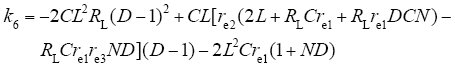
因本文欲通过小信号模型完成对变换器的闭环控制,只需求出该模型下电路输出变量vC1(s)、vC2(s)对控制变量d(s)的传递函数即可。为简化计算量,令N2 = N3 = N,C1 = C2 = C,L2 = L3 = N2L,忽略上式中与控制变量无关的部分并带入相关变量矩阵得到输出量对控制量的小信号传递函数

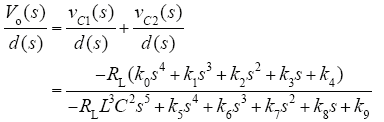
其中

3 电路闭环控制
3.1 系统框图分析
从建立的小信号模型式(11)可看出,系统对输出电压的控制不但由系统内各器件参数确定,工作过程中输入电压和负载这些外部扰动也会对系统输出环节的稳定性造成影响。因此,需对开关信号的占空比进行实时调节以平衡系统在工作过程中外部扰动对输出量造成的影响。将系统占空比作为设计变换器闭环系统的控制变量,系统的闭环环路框图如图4所示。
图4
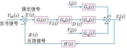
式(12)为图中系统回路增益函数,Gc(s)是误差E(s)到控制量Vc(s)的传递函数,即为本章将要设计的补偿网络传递函数。Go(s)为原始回路增益函数,表示控制信号Vc(s)至反馈信号B(s)间的传递函数。其中传函Gvd(s)为变换器开关占空比小信号变化量d(s)对变换器输出电压Vo(s)的传递函数,见式(11)。

式中,H(s)为反馈分压网络的传递函数,是对系统输出量的反馈采样;Gm(s)为PWM脉宽调制器的传递函数;Vm为PWM调制器中锯齿波幅值。将上述各环节结合得系统未补偿的原始回路增益函数
本设计在达到较高升压比的同时使电路反激变压器输出量及耦合电感输出量保持一致,以维持电路较高工作效率,选取系统额定工作参数见下表。
表 系统额定工作参数
Tab.
| 参数 | 取值 | 参数 | 取值 | |
|---|---|---|---|---|
| Vi/V | 5 | re1/Ω | 0.04 | |
| RL/Ω | 150 | re2/Ω | 0.5 | |
| fs/kHz | 20 | re3/Ω | 0.5 | |
| D | 0.5 | N1∶N2∶N3 | 1∶4∶4 | |
| L/μH | 210 | RL1/kΩ | 9 | |
| C/μF | 470 | RL2/kΩ | 1 | |
| Vo/V | 50 | Vm/V | 5 |

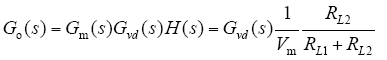
由式(14)得原始回路增益函数伯德图如图5所示,可明显看出,原始回路增益函数相位裕度偏小,且在截止频率处幅频特性曲线斜率大约为-40dB/dec,此时系统具有较大超越量和调节时间,系统的动态性能和稳定性较差。为使升压变换器系统满足稳定性要求,应对该函数进行校正使其相位裕度不低于45°,幅值裕度约为6dB左右。

图5
3.2 闭环控制系统设计
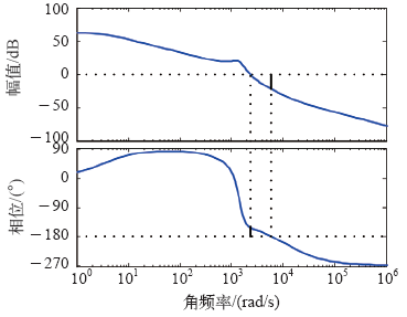
为保持系统输出环节稳定性,减少外部扰动对系统的影响,设计补偿网络对系统进行闭环调节。传统补偿网络可分为超前补偿网络、滞后补偿网络及超前–滞后补偿网络三种。超前网络可以提高系统的微分效应,对幅频斜率及相位裕度进行补偿;滞后网络易降低系统的开环截止频率,但可提高系统的相位裕度。综合该设计中需解决的问题,采用一种有源超前–滞后补偿网络对原始增益函数进行校正,该网络补偿器原理图如图6所示。
图6
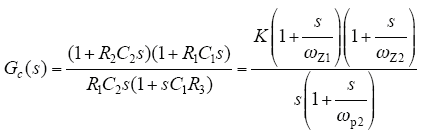
式(15)为网络补偿器传递函数,该补偿网络可在低频区提供一个积分环节以减少输出响应的调节时间,在中高频段滞后部分增加系统相位裕度,超前部分可使截止频率点右移来改善系统幅值裕度。
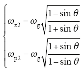
图7
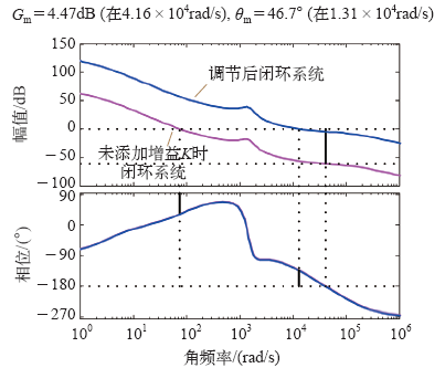
图7
闭环网络传递函数的伯德图
Fig.7
The Bode diagram of closed-loop transfer function network
令电阻R2 = 10kΩ,根据式(18)求出其他元件参数:R1 = 1.5kΩ,R3 = 25Ω,C1 = 0.4μF,C2 = 1μF。
由式(14)和式(18)得闭环网络传递函数

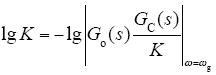
图7中红线为调节后闭环系统伯德图,调节后伯德图相位裕度r = 46.7°>45°,截止频率ωc = 1.31×10⁴rad/s与期望值基本一致,幅值裕度A(ω) = 4.47dB,满足系统静态和动态特性的要求。
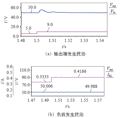
4 仿真及实验结果验证
4.1 仿真结果
为验证所提新型电路及变换器闭环控制系统设计的正确性,本文利用Saber仿真软件对集成耦合电感升压–反激变换器及闭环控制网络进行仿真,仿真和实验参数见上表。
图8
4.2 实验结果
为进一步证明理论分析的正确性及验证仿真结果的有效性,在实验室设计30W实验样机进行验证,如图9所示。样机中整流二极管使用肖特基二极管SR560,使用10kΩ贴片电阻及104贴片电容组成RCD滤波器并联在反激变压器一次侧。输出电容采用470μF电解电容,同时并联两个103贴片滤波电容。开关器件使用有源MOSFET芯片CSD17505,使用STM32F103RBT6作为控制芯片,其输出的PWM控制信号通过光耦TLP250来驱动开关的通断。
图9
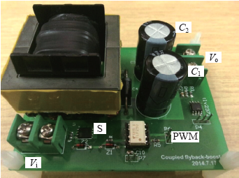
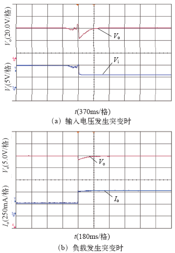
图10
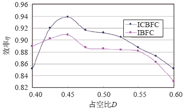
在验证电路闭环稳定性的同时,对各个占空比下ICBFC与IBFC工作效率进行测试并绘制曲线。可以看出ICBFC工作效率在D = 0.45时达到最大。由于利用反激变换器和耦合电感共同分担升压任务,因此在相同电压增益下,ICBFC中漏感总量较小,工作效率较IBFC要高。变换器在工作占空比D = 0.5左右可维持较高工作效率。
图11
5 结论
本文提出一种新型高电压增益的DC–DC变换器–集成耦合电感升压–反激变换器。分析了其工作原理及升压机理,针对集成耦合电感升压–反激变换器,在考虑元器件寄生参数的情况下利用状态空间平均法建立了相应小信号模型,通过对其幅频特性曲线的分析,设计了有源补偿网络对该变换器进行电压闭环控制,得到了理想的系统动、静态特性。
利用仿真软件及实验样机对闭环控制系统进行验证,证明了理论分析的正确性,对该变换器的操作和应用提供了理论依据。
参考文献
A front-end DC-DC converter for network server applications
[C].
High Performance Coupled-Inductor DC-DC Converter
[C].
A high efficiency flyback converter with new active clamp technique
[J].DOI:10.1109/TPEL.2010.2042302 URL [本文引用: 1]
High-efficiency, high step-up DC-DC converters
[J].
DOI:10.1371/journal.pone.0206691
URL
PMID:30500857
[本文引用: 1]

Over the past few years, high step-up dc-dc converters have been drawn substantial attention because of their wide-ranging application not only in the renewable energy sector but also in many other applications. To acquire a high voltage gain in photovoltaic (PV) and other renewable energy applications, a high step-up dc-dc converter is proposed in this paper. The proposed converter structure consists of a full-bridge (FB) module along with an input boost inductor and a voltage multiplier based on the Cockcroft-Walton (CW) principle with a parallel inductor. The key features of the proposed converter are: 1) high voltage gain with lower voltage stress on the switches, diodes and other passive elements without affecting the number of cascaded stages, 2) a minimum size of boost inductance and cascaded stage capacitance that ensures its compactness and low cost, and 3) a minimal number of major components. Circuit operation, steady-state analysis and various design parameters of the proposed converter are explained in details. In order to prove the performance of the theoretical analysis, a laboratory prototype is also implemented. The peak voltage gain and the maximum efficiency obtained are 11.9 and 94.6% respectively with very low input current ripple and output voltage ripple generated.
Analysis of integrated boost-flyback step-up converter
[J].DOI:10.1049/ip-epa:20045003 URL [本文引用: 1]
Aggregated modeling and control of integrated boost-flyback high step-up converter
[C].
An input current shaper with boost and flyback converter using integrated magnetics
[C].
Interleaved boost-flyback converter with boundary conduction mode for power factor correction
[C].
Series- connected forward-flyback converter for high step-up power conversion
DOI:10.1109/TPEL.2011.2162747
URL
[本文引用: 1]
Recently, small-scale and highly-distributed photovoltaic power sources have been researched for the high generation efficiency even under severe partial shading conditions. However, power conditioning systems for the sources needs high step-up voltage gain due to the low output of the generating sources. This paper presents a newly-suggested high step-up topology employing a Series-connected Forward-FlyBack (SFFB) converter, which has a series-connected output for high boosting voltage-transfer gain. SFFB is a hybrid type of forward and flyback converter, sharing the transformer for increasing the utilization factor. By stacking the outputs of them, extremely high voltage gain can be obtained with small volume and high efficiency even with a galvanic isolation. The separated secondary windings in low turn-ratio reduce the voltage stress of the secondary rectifiers, contributing to achievement of high efficiency. The single-ended scheme is also beneficial to the cost competitiveness. In this paper, the operation principle and design guidelines of the proposed scheme are presented, along with the performance analysis and numerical simulation. Also, a 100 W SFFB DC/DC converter hardware prototype has been implemented for experimental verification of the proposed converter topology.
Improved integrated boost-flyback high step-up converter
[C].
Analysis and implementation of interleaved single-stage single-phase AC-DC boost-flyback converter
[C].
基于switch-capacitor网络的单开关升压变换器
[J].
A single-switch step-up converter based on switch-capacitor network
[J].
基于拓扑组合的高增益Boost变换器
[J].The high step-up Boost converter based on topology combination is proposed in this paper. The operation principle and property of the converter are analyzed in detail. The experimental results are given. When duty ratio D>0.5, the converter has these characteristics as follows: Firstly, the voltage gain is double of the basic Boost converter. Secondly, the two Boost cell of the converter can realize current sharing automatically, which is unlike the interleaved Boost converter, and therefore, the control circuit is simple. Finally, the voltage stress of the active switch is half of the output voltage, namely, it is half of the voltage stress of the basic Boost converter.
High step-up boost converter based on topology combination
[J].The high step-up Boost converter based on topology combination is proposed in this paper. The operation principle and property of the converter are analyzed in detail. The experimental results are given. When duty ratio D>0.5, the converter has these characteristics as follows: Firstly, the voltage gain is double of the basic Boost converter. Secondly, the two Boost cell of the converter can realize current sharing automatically, which is unlike the interleaved Boost converter, and therefore, the control circuit is simple. Finally, the voltage stress of the active switch is half of the output voltage, namely, it is half of the voltage stress of the basic Boost converter.
